Ongoing Projects
Laser-assisted Atomic Layer Etching of Semiconductors and Nanomaterial
Sponsor: NSF/CMMI
TMDC layer thinning by apertureless tip-based process
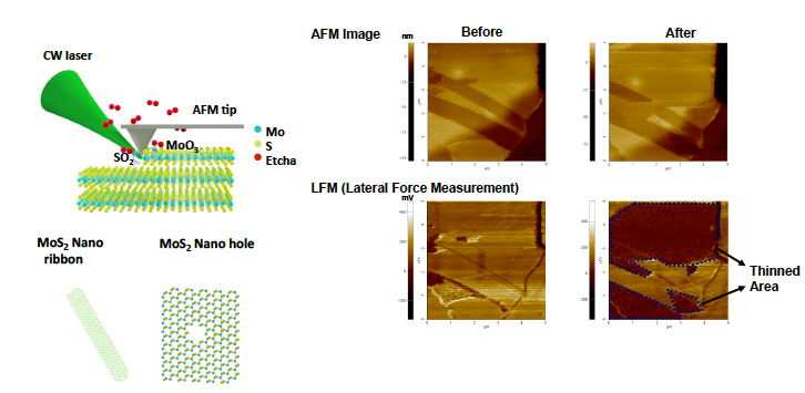
Laser-assisted chemical etching can control the removal of an ultra-thin layer of material using sequential self-limiting reactions. The combination of surface processing experiments with analytical diagnostics bridges a scientific gap in the understanding of ALEt mechanisms that so far have not received detailed scrutiny and analysis. The research will examine the dissociation of precursor etchant gases by applying ultraviolet laser sources under different pressures and flow rates, measure and correlate the concentrations of the produced radicals to the surface coverage. Work will be conducted to investigate the effect of laser-induced excitation of the target material and the adsorbed atoms on the atomic layer removal under different incident irradiation wavelengths, pulse durations and energy densities. The laser-aided ALEt concept will be extended to accomplish layer-by-layer etching of transition metal dichalcogenide (TMDC) films and graphene via tip-based nanopatterning. On-line spectroscopy will probe the mechanisms of the laser-induced dissociation process, the coupling of the processing laser to the target material and the desorption process. The laser activation of ALEt will also be explored as a means to establish a low temperature etching process compatible and complementary to plasma-mediated processes.
Microscopic mechanisms and kinetics of laser-induced phase explosion
Sponsor: NSF/CBET
Collaborator: Leonid Zhigilei, University of Virginia
Collaborator: Leonid Zhigilei, University of Virginia
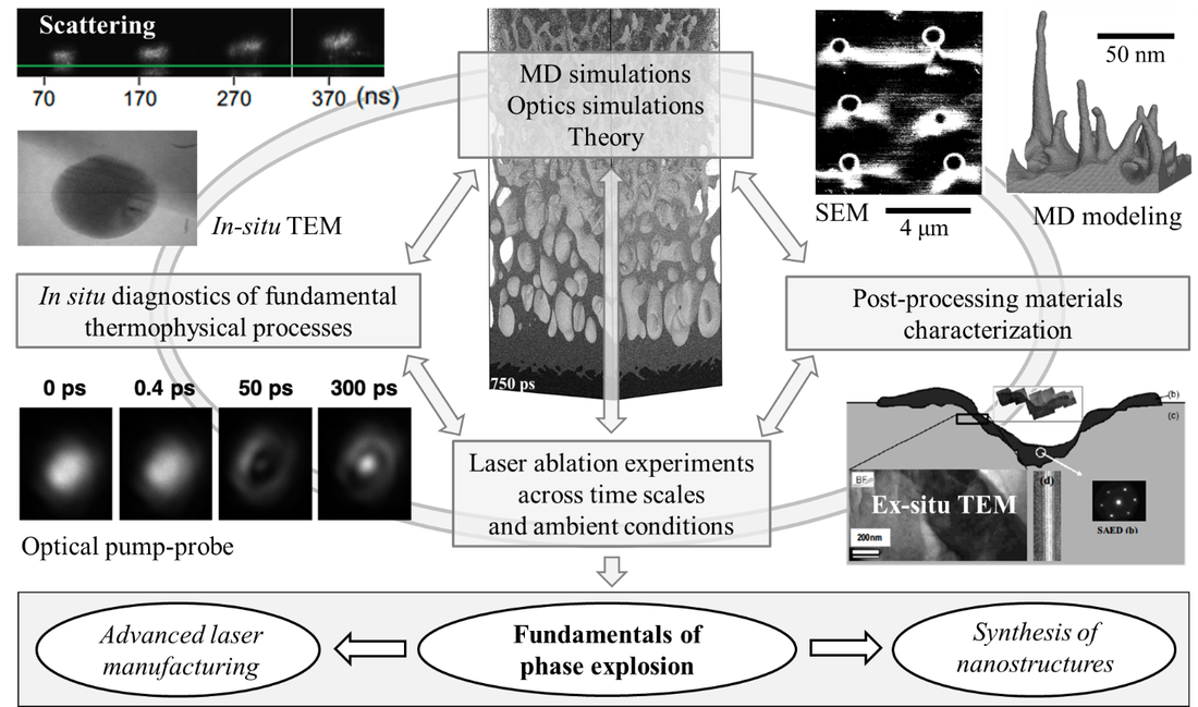
Conceptual diagram of the research on laser-driven phase explosion
The mode of vaporization that occurs through a massive homogeneous nucleation of vapor bubbles in a volume of the strongly superheated liquid, called “explosive boiling” or “phase explosion,” is a common phenomenon that plays a key role in numerous practical applications ranging from generation of nanoparticles and nanomaterials to surface cleaning and nano/microfabrication. Despite decades of extensive experimental and theoretical studies, a clear understanding of the conditions and microscopic mechanisms of the phase explosion is still lacking. The objective of the research program is to gain a solid understanding of the mechanisms and kinetics of the explosive phase decomposition in a metastable liquid superheated up to the limit of its thermodynamic stability by short pulse laser irradiation. A combination of large-scale atomistic simulations with time-resolved probing of the transient dynamics of the phase explosion will be used to track all stages of the process, from the emergence of the density fluctuations, to the formation and coarsening of distinct liquid regions, and to disintegration of the continuous liquid foamy structure into individual liquid droplets. The dependence of the dynamics of the phase explosion on the environment, geometry of the target, and the heating rate will be investigated to gain further insights into the fundamental mechanisms and to enable control over the process for practical applications.
In-situ TEM holder for ultrafast, multimodal imaging
Sponsor: DOE/BES
Collaborators: Andrew Minor (UCB MSE), Laser Prismatics
Collaborators: Andrew Minor (UCB MSE), Laser Prismatics
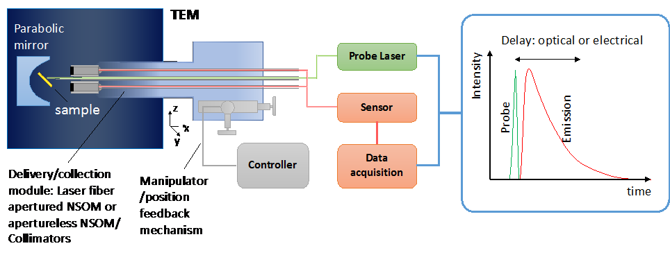
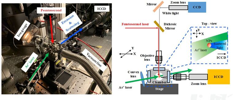
Overall schematic of the experimental apparatus for in-situ multimodal optical spectroscopy.
Many energy conversion and transfer processes critically depend on the material nanostructure details and its response to external excitation fields. Surface and volume defect formation and migration have a profound impact on the opto-electro-thermo-mechanical properties of materials. Understanding these processes requires a unique combination of advanced atomic-scale imaging with controlled nanoscale excitation and quantitative probing of fundamental processes. This project is therefore focused on simultaneous nanoscale multimodal imaging of energy conversion/transfer processes by integrating tip-based pulsed laser radiation sources within a transmission electron microscope (TEM). Nanoscale confinement of radiation fields of enhanced intensity underneath a tip-based probe enables unambiguous and direct in-situ interrogation of the nanostructure effects on the material properties. We have already demonstrated proof-of-principle experiments using a lensed-optical fiber in a scanning electron microscope (SEM) and the initial fabrication of a fiber-optic manipulation TEM holder. This project brings this concept to the next level into a tangible product, where integration of a near field scanning optical microscopy (NSOM) fiber into a TEM will allow for direct imaging of the microstructural response of materials undergoing optical excitation, possibly also in the presence of external radiative, thermal, electrical and mechanical force fields. Even though optical imaging techniques offer convenient in-situ monitoring, their spatial resolution is not sufficient for inspecting detailed phenomena occurring in micro/nano structures. Similarly, ex-situ electron microscopy studies (using “before” and “after” images) are impractical for truly nanoscale spectroscopic techniques, and do not provide the depth of understanding that live in-situ imaging can offer.
Tip-Based Femtosecond Multiphoton Spectroscopy with Radiative Heating
Sponsor: DOE/BES
Collaborators: Andrew Minor, Lane Martin (UCB MSE), Laser Prismatics
Collaborators: Andrew Minor, Lane Martin (UCB MSE), Laser Prismatics
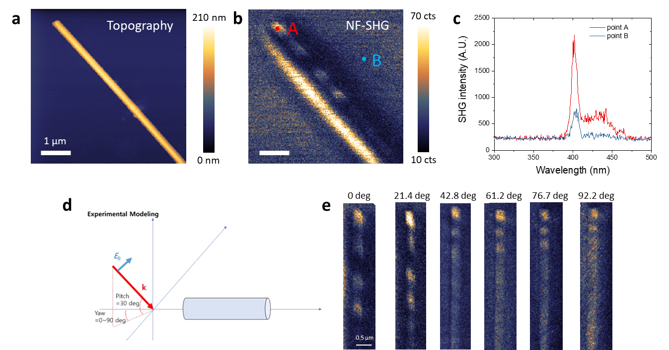
a) Topography of Si NW, b) corresponding NF-SHG mapping images and c) Spectral intensity obtained from A and B point indicated in panel b)
One of grand challenges in nanoscience and nanotechnology is to achieve fundamental understanding of the dynamic evolution of materials in actual operating environment, non-equilibrium conditions, or undergoing chemical reactions at the nanoscale. This requires forefront advances in imaging and analysis techniques that combine nanometer-scale spatial resolution, optical excitation and spectroscopic detection for direct in-situ observation of the fundamental processes. Our in-situ nanoscale imaging method integrates tip-based near-field scanning optical microscopy with femtosecond multiphoton spectroscopy. The main outcome of this project is the development of a flexible nanoscale imaging instrument capable of in operando nanoscale imaging.
3D Microstructuring
Sponsor: NSF/CMMI
Collaborators: Phillip Marcus (UC Berkeley), Kyriakos Komvopoulos (UC Berkeley), Grace X. Gu (UC Berkeley), Maria Farsari (FORTH GREECE)
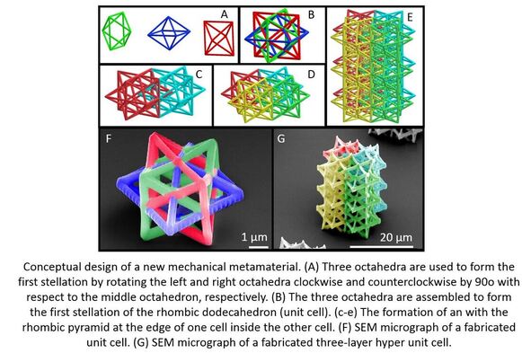
Multiphoton Lithography enables the design of complex structures with nano or microscale features. These structures have proved to provide unprecedented properties in the structures, superseding the limitations of the initial bulk materials. Comprehending the mechanical response that is evinces is imperative to provide a coherent framework for the design of these structures.
This objective of this project is to delineate the design principles and the mechanical behavior that must be substantiated to accomplish the tailored performance of architected geometries.
This objective of this project is to delineate the design principles and the mechanical behavior that must be substantiated to accomplish the tailored performance of architected geometries.
Laser-Chemical Processing of Semiconductor Devices Based on Two Dimensional Atomic Layer Material
Sponsor: NSF/CMMI
Collaborators: Junqiao Wu (UC Berkeley)
Collaborators: Junqiao Wu (UC Berkeley)
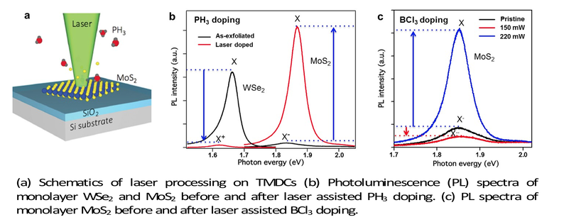
Two dimensional atomic layer semiconductors based on transition metal dichalcogenides have attracted intense interest due to their exceptional optoelectronic characteristics. Laser-assisted chemical processing has substantial potential to overcome these limitations and accomplish stable nanomanufacturing of atomic layer semiconductor devices. This award investigates new methods to fabricate high-performance devices with ultra-high sensitivity and extraordinary functionalities.The project contributes a new technology for the processing, functionalization and patterning of transition metal dichalcogenide-based two dimensional semiconductors. The chemical composition of these two dimensional semiconductor materials will be modified and controlled at the nanoscale by incorporating foreign atoms from a selected gas source by means of laser irradiation. This process is stable in ambient air with respect to time and enables precise tuning of the electronic characteristics of the material that is necessary for fabricating high performance devices.
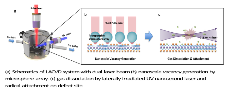
The core objective of this project is to utilize laser driven chemical processing for localized functionalization of two dimensional atomic layer semiconductors. To accomplish this goal, a dual beam processing system is studied. The processing system is comprised of a beam irradiated at normal incidence for the generation of vacancies and another synchronized ultraviolet nanosecond laser beam irradiated parallel to the target specimen for dissociation of dopant precursor gas molecules. In this manner, it is possible to decouple and control the mechanisms involved in the doping and alloying processes. Aiming at reducing feature resolution and generating highly defined nanoscale patterns, near field optical processing is implemented. The functionality of the laser-processed materials is demonstrated through designing, fabricating and testing devices that highlight the modified and tuned material transport characteristics and optoelectronic responses. The scalability and integration to functional devices is explored in order to incorporate the developed concepts into large-scale production. The first breakthrough entails stable and spatially controlled writing of p- and n-doped domains in these materials and is followed by the deliberate tuning of the semiconductor band gap via laser induced alloying. The second major contribution from a nanomanufacturing perspective is the direct nanopatterning of the target materials by using assembled microlens and nanowire elements that are integrated into the laser chemical vapor deposition apparatus. The research work is validated by fabricating transistors having sharp nanoscale PN junctions and lateral tandem optoelectronic devices. Finally, this project offers a robust and repeatable platform for discovering entirely new and exciting physics of these exotic materials.
The core objective of this project is to utilize laser driven chemical processing for localized functionalization of two dimensional atomic layer semiconductors. To accomplish this goal, a dual beam processing system is studied. The processing system is comprised of a beam irradiated at normal incidence for the generation of vacancies and another synchronized ultraviolet nanosecond laser beam irradiated parallel to the target specimen for dissociation of dopant precursor gas molecules. In this manner, it is possible to decouple and control the mechanisms involved in the doping and alloying processes. Aiming at reducing feature resolution and generating highly defined nanoscale patterns, near field optical processing is implemented. The functionality of the laser-processed materials is demonstrated through designing, fabricating and testing devices that highlight the modified and tuned material transport characteristics and optoelectronic responses. The scalability and integration to functional devices is explored in order to incorporate the developed concepts into large-scale production. The first breakthrough entails stable and spatially controlled writing of p- and n-doped domains in these materials and is followed by the deliberate tuning of the semiconductor band gap via laser induced alloying. The second major contribution from a nanomanufacturing perspective is the direct nanopatterning of the target materials by using assembled microlens and nanowire elements that are integrated into the laser chemical vapor deposition apparatus. The research work is validated by fabricating transistors having sharp nanoscale PN junctions and lateral tandem optoelectronic devices. Finally, this project offers a robust and repeatable platform for discovering entirely new and exciting physics of these exotic materials.
SNM: High-Throughput Scalable Nanomanufacturing of High-Performance Organic Devices
Sponsor: NSF/CMMI
Collaborators: Adam Moulé(PI), Mark Mascal (UC Davis), Alberto Salleo (Stanford), Palo Alto Research Center (PARC)
Collaborators: Adam Moulé(PI), Mark Mascal (UC Davis), Alberto Salleo (Stanford), Palo Alto Research Center (PARC)
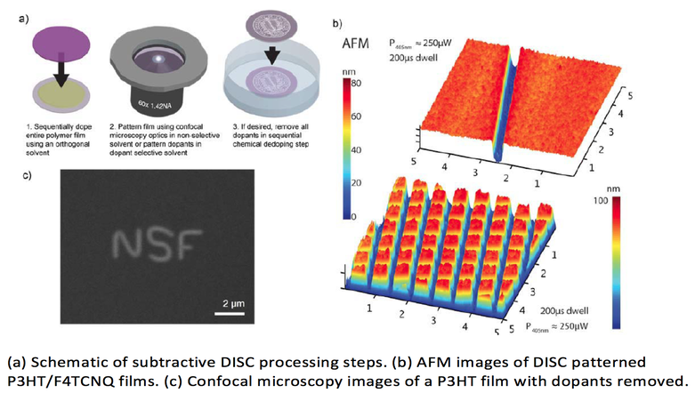
A significant obstacle for the development of organic devices is the lack of a patterning technology with the disruptive power that photolithography exerted in traditional microelectronics. There is therefore a critical need to develop and scale-up photopatterning methods capable of patterning organic semiconducting with sub-micrometer resolution. The long-term goal of this work is to use a series of sequential processing steps to fabricate nanoscale multi-layer organic electronic devices. Here we introduce a new scalable patterning technology for organic semiconductors called dopant-induced solubility control (DISC) that takes advantage of the existing photolithography infrastructure and is compatible with digital direct-write patterning and sequential roll-to-roll (R2R) solution coating. DISC processing steps can be applied sequentially to deposit and pattern multiple layers of electronically active polymers with sub-micrometer features without causing impairment of functionality. We will use these steps to fabricate large arrays of all organic thin-film transistors with doped polymers for electrodes, channel lengths of <500 nm, and layer registration in the 10s of nm that have switching speeds in the 100s of MHz.
Collaborative Research: Engineering Human 3D Cardiac Tissue Model of Hypertrophic Cardiomyopathy
Sponsor: NSF/EBMS
Collaborators: Zhen Ma (Syracuse University)
Collaborators: Zhen Ma (Syracuse University)
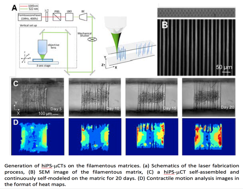
Currently, human induced pluripotent stem cell (hiPSC) technology has provided previously unanticipated possibilities to model human heart diseases in cell culture as “disease-in-a-dish”. However, the grand challenge in current hiPSC disease modeling is that these models have tended to simplify the diseases as monogenic, hereditary forms of diseases, which could not recapitulate the diversity in disease phenotypes resulting from genetic-environmental interactions. Specifically, hypertrophic cardiomyopathy (HCM), the leading cause of sudden cardiac death among young adults and athletes, indicates that physical stress increases the risk of developing heart failure in the patients with HCM-related genetic predispositions. Therefore, to develop useful in vitromodel systems for identifying the correlation between genetic deficiencies and environment stresses, it is necessary to precisely control the environmental stress exerted on hiPS-derived cardiac microtissues (hiPS-µCTs). This work focuses on the MYBPC3 gene, one of the most frequent mutated HCM genes, while molecular mechanisms by which MYBPC3 mutations lead to HCM remain elusive. The primary goal of this proposal is to investigate the correlation between HCM phenotypes and dose-dependent reduction of MYBPC3 expression (haploinsufficiency), and how it could be exacerbated by the increase of environmental stress to the hiPS-µCTs.
Key to the success of this effort is encompassing both synthetic and biological approaches to create a disease-specific, functional 3D cardiac tissue model de novo, which offers better understanding of how the genetic defects interplay with the cellular and tissue environment to initiate and progress the cardiac diseases. This model will represent a significant advancement for investigating genotype-phenotype correlation associated with the clinical heterogeneity, elucidating the disease progression in human cardiomyopathies, and developing new therapeutic strategies for disease management and treatment.
Key to the success of this effort is encompassing both synthetic and biological approaches to create a disease-specific, functional 3D cardiac tissue model de novo, which offers better understanding of how the genetic defects interplay with the cellular and tissue environment to initiate and progress the cardiac diseases. This model will represent a significant advancement for investigating genotype-phenotype correlation associated with the clinical heterogeneity, elucidating the disease progression in human cardiomyopathies, and developing new therapeutic strategies for disease management and treatment.
Recently Completed
Ultrafast Laser Processing
Sponsor: Samsung
Patterning of target materials through the laser ablation is a highly promising technology since it reduces the manufacturing costs due to the number of processing procedures that conventional chemical etching methods require. In addition, it also provides various aspects of patterned features depending on the imparted laser light sources. More specifically, the femtosecond laser is highly effective, since it can reduce the molten traces, such as droplet finger or re-solidified rims. The purpose of this work is to investigate the evinced physical mechanisms that cause different morphologies due to femtosecond laser ablation.
SNM: Scalable Three-Dimensional Nanomanufacturing Combining Ultrafast Laser Processing and Directed Self-Assembly
Sponsor: NSF/EEC
Collaborators: Thomas P. Russell (U. Mass., Amherst), David Dornfeld, Xiang Zhang (UCB), Maria Farsari (IESL/FORTH, Greece)
Collaborators: Thomas P. Russell (U. Mass., Amherst), David Dornfeld, Xiang Zhang (UCB), Maria Farsari (IESL/FORTH, Greece)
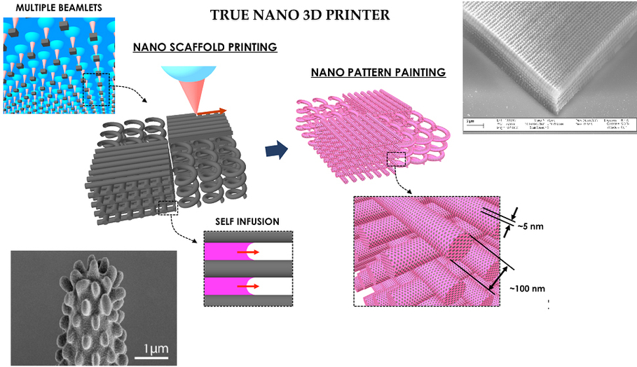
Nanomaterials and nanotechnology offer unique opportunities for fabricating devices of novel architecture and enhanced performance and can overcome system integration issues challenging current nanomanufacturing methods that are suited to planar geometries and are confined to top-down architectures. The central motivation of this work is to develop a new manufacturing paradigm that offers scalability and flexibility enabling nanoscale device fabrication and integration in truly three-dimensional architectures over large areas and with arbitrary densities. A robust, fully proven and scalable platform for building nanosystems of unprecedented sensitivity and functionality will be developed. The research will have an impact on education and the development of transformational and sustainable nanomanufacturing technology while broadening our understanding of the fundamental science. Applications include advanced optical materials, high sensitivity sensors and nanomaterials for tissue engineering.
The core research strategy takes advantage of ultrafast laser beam processing for generating the scaffold multi-scale structures with sub-50 nm feature resolution. Two-photon polymerization will be used to fabricate structures of tunable properties that are sensitive to pressure, light, heat and electrical stimulation. This technique, together with ultrafast laser micro/nanomachining will be adapted to multiple beam configurations in order to increase the processing throughput. Once the template is constructed, the directed self-assembly of block copolymers will be used to produce three-dimensional materials with tailored functionality where pattern amplification will be used to push the length scale to the sub-10 nm regime. The directed self-assembly of block copolymers is a parallel process and, as such, particularly over the fundamental length scales of concern in these studies, is quite rapid. Direct laser writing will be used to create structures of the desired structural properties, including optical waveguides, fluidic channels and conductive circuitry. The following examples of functional structures will be demonstrated: i) highly sensitive three-dimensional multi-plexed sensor devices, ii) large area complex three-dimensional metamaterials and iii) nanostructured tissue scaffolds. The impact of materials and chemicals, consumption of energy and other resources during manufacturing, as well as product end-of-life and recycling will be evaluated in a sustainability analysis.
The core research strategy takes advantage of ultrafast laser beam processing for generating the scaffold multi-scale structures with sub-50 nm feature resolution. Two-photon polymerization will be used to fabricate structures of tunable properties that are sensitive to pressure, light, heat and electrical stimulation. This technique, together with ultrafast laser micro/nanomachining will be adapted to multiple beam configurations in order to increase the processing throughput. Once the template is constructed, the directed self-assembly of block copolymers will be used to produce three-dimensional materials with tailored functionality where pattern amplification will be used to push the length scale to the sub-10 nm regime. The directed self-assembly of block copolymers is a parallel process and, as such, particularly over the fundamental length scales of concern in these studies, is quite rapid. Direct laser writing will be used to create structures of the desired structural properties, including optical waveguides, fluidic channels and conductive circuitry. The following examples of functional structures will be demonstrated: i) highly sensitive three-dimensional multi-plexed sensor devices, ii) large area complex three-dimensional metamaterials and iii) nanostructured tissue scaffolds. The impact of materials and chemicals, consumption of energy and other resources during manufacturing, as well as product end-of-life and recycling will be evaluated in a sustainability analysis.
Directed Templating of Semiconductor Nanocrystals Through Laser Melting
Sponsor: NSF/CMMI
Collaborators: Heng Pan (Missouri UST), Andrew M. Minor (UCB)
Collaborators: Heng Pan (Missouri UST), Andrew M. Minor (UCB)
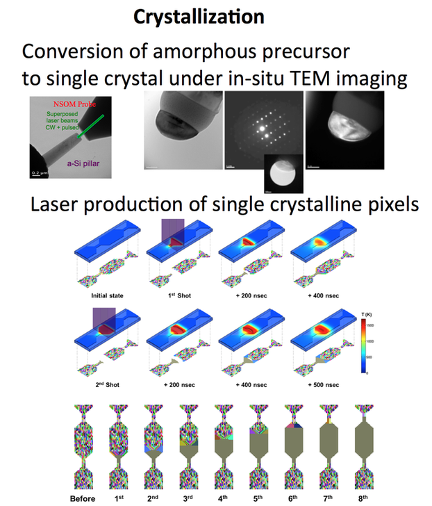
Control of nucleation to drive crystal growth of high quality is important for many applications in photonic and electronic devices. The essential, but still challenging step is the deliberate templating of nanocrystals with the desired size and orientation into heterogeneous substrates. Once these are defined, it is possible to devise fabrication routes for different device architectures at the nanoscale or the microscale. Ordered arrays of quantum array semiconductors can be fabricated for integration into quantum nanodevices. Furthermore, the nanocrystals serve as seeds for promoting growth of crystalline material.
In this project, we seek to manufacture nanocrystal seeds with highly uniform size and orientations by laser crystallization in confined nanodomains. We achieve fundamental understanding of laser crystallization in nanodomains by combining direct imaging via in situ Transmission Electron Microscopy (TEM) with detailed multi-scale computational modeling and molecular dynamic (MD) simulations. This uniquely integrated research approach can provide sufficiently detailed understanding such that we can engineer the nanoconfinement geometry and the imposed transient laser protocol parameters for reliable generation of well-controlled seeding nanocrystals. State of the art focused ion beam (FIB) processing and laser interference lithography are being utilized to define nanocavities with minimum diameter <10 nm wherein amorphous semiconductors (Si, Ge) will be deposited. The nanocavity fabrication on large area can be achieved by nanoimprinting with FIB fabricated molds in a repeatable manner for industrial scale manufacturing. Pulsed laser radiation in combination with modulated background heating is utilized to convert the amorphous deposits into nanocrystals with deliberately engineered size and crystallographic orientation. Such generated localized crystals can serve as crystallization seeds, hence offering great engineering value for overcoming uncertainty associated to un-engineered spontaneous nucleation. Finally, we propose a seeded crystallization process enabling controlled growth of a monocrystalline thin layer in a large scale on epitaxially non-participating transparent substrates. The innovative concept of decoupling seed formation from subsequent crystal growth along with the unprecedented investigation approach will lead to a revolutionary solution that semiconductor manufacturing industry has been pursuing for years.
The research establishes an integrated approach for seamlessly connecting fundamental understanding of nanoscale nucleation and crystallization to the rational design of seeded and directed thin film crystal growth methods. Success of this project will open the way to the fabrication of thin crystalline domains on inexpensive, non-epitaxial substrates as well to the fabrication of quantum nanodevices. Many critical applications will benefit from this work, including quantum computers, TFTs for advanced displays, high performance thin film solar cells, and 3-D electronic devices.
Flexible 2D RF Nanoelectronics based on Layered Semiconductor Transistor
Sponsor: AFOSR/AOARD
Collaborators: Sunkook Kim (Kyung Hee University, S. Korea) , Woong Choi (Kookmin University, S. Korea)
Collaborators: Sunkook Kim (Kyung Hee University, S. Korea) , Woong Choi (Kookmin University, S. Korea)
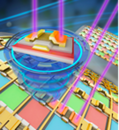
Extensive technological progress has been achieved in the field of ‘flexible/stretchable electronics’, including flexible displays, human-inspired electronics, and wearable electronics. Molybdenum disulfide (MoS2), composed of vertically stacked layers held together by van der Waals interactions, is drawing attention as a promising alternative to silicon-based electronics. MoS2 TFTs exhibit exceptional characteristics: relatively large bandgap (1.2-1.9 eV), high mobility at room temperature (up to ~ 500 cm2V-1s-1), low subthreshold swing (SS, ~70 mV decade-1), high on/off ratios (~107), and potential amenability to a low-cost, large-area growth technique such as chemical vapor deposition (CVD).
However, there are several key challenges that lie ahead before the transistors based on 2D layered semiconductors can be integrated into flexible/stretchable circuits. The key challenges include inaccessibility of large area growth/coverage of layered semiconductors, non-uniformity between devices, high contact resistance between metal electrodes and semiconductors, and the system integration with flexible substrates. Computational and experimental studies in multidisciplinary fields of electrical, mechanical engineering, and materials science are being pursued to achieve: (i) formation of 2D layered semiconductor over large-area substrates with good control of thickness, crystal structure, and defects; (ii) development of laser annealing for reducing contact resistance and crystallization of amorphous TMDs (MoSe2 / MoS2) for high-mobility TFTs (>70 cm2 V− 1s− 1); (iii) development of unit processes (e.g. gate dielectrics, passivation, flexible substrate) for flexible TFTs; (iv) optimization of device designs to achieve RF transistor, and develop RF device model
However, there are several key challenges that lie ahead before the transistors based on 2D layered semiconductors can be integrated into flexible/stretchable circuits. The key challenges include inaccessibility of large area growth/coverage of layered semiconductors, non-uniformity between devices, high contact resistance between metal electrodes and semiconductors, and the system integration with flexible substrates. Computational and experimental studies in multidisciplinary fields of electrical, mechanical engineering, and materials science are being pursued to achieve: (i) formation of 2D layered semiconductor over large-area substrates with good control of thickness, crystal structure, and defects; (ii) development of laser annealing for reducing contact resistance and crystallization of amorphous TMDs (MoSe2 / MoS2) for high-mobility TFTs (>70 cm2 V− 1s− 1); (iii) development of unit processes (e.g. gate dielectrics, passivation, flexible substrate) for flexible TFTs; (iv) optimization of device designs to achieve RF transistor, and develop RF device model
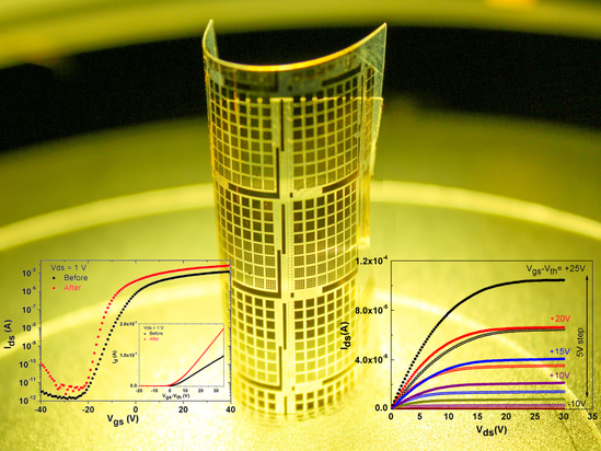
The typically used substrates (e.g. PEN, PET, and PI) for flexible applications pose significant manufacturing challenges, since the fabrication sequence must have a low thermal budget (< 200 °C). Therefore, conventional high thermal annealing processes cannot be applied as they affect the entire panel, including unwanted areas where the annealing process should be excluded. The irradiation of a pulsed laser with high energy density and short wavelength onto the metal electrode leads to thermal annealing effect at the locally confined small area that needs high temperature without severe thermal damage. We report the use of ultra-short, pulsed-laser annealed Ti/Au contacts to enhance the performance of multilayer MoS2 field effect transistors (FETs) on flexible plastic substrates without thermal damage. The reduced contact resistance after laser annealing provided a significant improvement in transistor performance including higher peak field-effect mobility, increased output resistance, a six-fold increase in the self-gain, and decreased subthreshold swing.
Maskless Fabrication of Electronics and Energy Devices
Sponsor: NSF, KAUST, Laser Prismatics, SinBeRISE
Collaborators: Seung-Hwan Ko (Seoul National University), Daeo Lee (Gachon University) Andrew M. Minor (UCB), Hee K. Park (Laser Prismatics)
Collaborators: Seung-Hwan Ko (Seoul National University), Daeo Lee (Gachon University) Andrew M. Minor (UCB), Hee K. Park (Laser Prismatics)
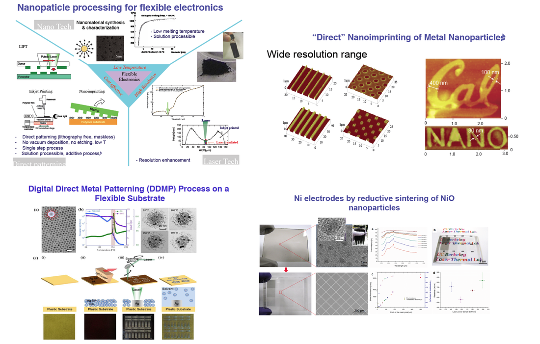
Electric circuit fabrication on polymer substrate is being referred to as “flexible electronics” and has gained significant interest as a pathway to low cost or large area electronics. The main goal of this evolving work is to achieve functionalization of nanostructrures to high performance components with low thermal budget that is compatible with heat-sensitive, polymeric substrates. This research can be applied to systems requiring low cost, high resolution, lightweight, flexibility and portability without using conventional vacuum or photolithographic processes.
The Laser Thermal Laboratory has demonstrated a series of novel approaches to realize flexible electronics combining laser processing, inkjet printing and nanoimprinting for the maskless fabrication of electronic and energy devices. High performance all printed transistors have for example been fabricated.
Continuous (CW), temporally modulated and pulsed laser radiation is applied to functionalize deposited nanoparticle (NP) suspensions. Conductive paths are established through metal NP sintering at low temperatures. The process is conducted at low temperature due to the substantial melting point depression with diminishing NP size. Furthermore, laser radiation is used to anneal ZnO NPs to fabricate transparent electrodes and active devices. Recent work has focused on the fabrication of electrodes through the reductive sintering of metal oxide NPs (e.g. NiO and CuO) and the plasmonic sintering of nanowires (NWs). Practical applications on touch panel devices, storage devices, and displays are being pursued. The research has a strong fundamental component aimed at understanding nanostructuring and nanoscale phase transformations through in-situ imaging, time-resolved spectroscopic probing and theoretical modeling.
